Cygnet is a low-cost embeddable STM32L4-based microcontroller board designed to accelerate the development and deployment of battery-powered IoT solutions.
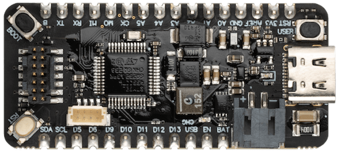
As a lower-cost alternative to the Swan, Cygnet still provides an extensive feature set required for edge-based inferencing and remote monitoring applications. Like its more expensive sibling, Cygnet is designed to be the ideal companion to Notecard while offering a more budget-friendly option.
Functional Description
Cygnet is a Feather-compatible STM32-based MCU, and a lower-cost alternative to our popular Swan MCU. Like the Swan, Cygnet is offered in a Feather standard form factor and uses a STM32L4 part while still providing plenty of flash and RAM to run the majority of your Notecard-powered applications.
Features
-
Features of the ST STM32L433CC microcontroller
-
80MHz Clock speed
-
256KB Flash, proprietary code readout protection
-
64KB of SRAM including 16KB with hardware parity check
-
Ultra-low-power with FlexPowerControl
-
11x timers
-
16x communication interfaces
-
14-channel DMA controller
-
Rich analog peripherals (independent supply)
-
True random number generator
-
-
Compliant with the Adafruit Feather Specification
-
Includes a USB-C port for easy power and serial connectivity
-
Includes a PMIC accessible via a JST PH connector, allowing you to either power the board via a LiPo battery and/or recharge the battery via USB.
-
-
USER_BTNprogrammable button -
LED_BUILTINprogrammable LED (red) -
JTAG (SWD capable) debug jack
-
BOOT and RESET buttons
-
Modular design supports Feather pins or an expansion PCB (to break pins out to 0.1" headers for easier wiring and debugging).
-
10kΩ pull-ups on the
SDAandSCLpins -
Qwiic connector
Package Configuration
The Cygnet can be used as a Feather-compatible board with soldered male headers, as a part of the Blues Notecard Feather dev kit.
Feather-compatible Cygnet
Out of the box, the Cygnet is usable as a Feather-compatible device.

Pin Information
The following tables contain pin definition mappings between the Cygnet Feather pins to the STM32L433 core MCU.
Cygnet Feather to STM32 Mapping
| Pin # | Pin Name | Pin # | Pin Name | |
|---|---|---|---|---|
| RST | RST# | ---- | ||
| 3V3 | ---- | |||
| AREF | ---- | |||
| GND | ---- | |||
| PA0 | A0 | BAT | ||
| PA1 | A1 | PH0 | EN | |
| PA2 | A2 | PB3 | USB | |
| PA3 | A3 | PB4 | D13 | |
| PB1 | A4 | PB15 | D12 | |
| PA7 | A5 | PB0 | D11 | |
| PA5 | CK | PB13 | D10 | |
| PB5 | MO | PB14 | D9 | |
| PA6 | MI | PB9 | D6 | |
| PA10 | RX | PB8 | D5 | |
| PA9 | TX | PB6 | SCL | |
| PH3 | B | PB7 | SDA | |
| PC13 | USER_BTN | PA8 | LED_BUILTIN |
Pin Description Table
| Pin Name | Pin Description (Primary) | Voltage Tolerance |
|---|---|---|
| A0 | I/O - GPIO, PWM, ADC | 5V |
| A1 | I/O - GPIO, PWM, ADC | 5V |
| A2 | I/O - GPIO, PWM, ADC | 5V |
| A3 | I/O - GPIO, PWM, ADC | 3.6V |
| A4 | I/O - GPIO, PWM, ADC | 5V |
| A5 | I/O - GPIO, ADC | 5V |
| D5 | I/O - GPIO | 5V |
| D6 | I/O - GPIO | 5V |
| D9 | I/O - GPIO, PWM | 5V |
| D10 | I/O - GPIO, ADC | 5V |
| D11 | I/O - GPIO, PWM, ADC | 5V |
| D12 | I/O - GPIO, PWM, ADC | 5V |
| D13 | I/O - GPIO, ADC | 5V |
| SCL | I²C - Serial Clock | 5V |
| SDA | I²C - Serial Data | 5V |
| 3V3 | Power - Constant 3.3V Supply | - |
| EN | Power - Chip Enable | 5V |
| GND | Power - Ground | - |
| RST | Power - Reset | - |
| BAT | Power - Battery Voltage Supply | - |
| AREF | Power - Reference Voltage | - |
| USB | Power - USB Voltage Supply | - |
| RX | Serial - Receive | 5V |
| TX | Serial - Transmit | 5V |
| B | Boot0 - Boot into Bootloader | 5V |
| MI | SPI - Main In Secondary Out | 5V |
| MO | SPI - Main Out Secondary In | 5V |
| CK | SPI - Serial Clock, DAC | 3.6V |
| ENABLE_3V3 | Enable External 3V3 Regulator | - |
| LED_BUILTIN | Built-in LED | - |
| USER_BTN | User Button | - |
NOTE: All digital I/O pins are interrupt capable.
Specifications
Electrical Characteristics
DC Characteristics
| Description | Minimum | Maximum | Unit |
|---|---|---|---|
VIN Supply Voltage | 2.5 | 5.5 | V |
VBAT Supply Voltage | 2.5 | 5.5 | V |
VUSB Supply Voltage | 2.5 | 5.5 | V |
| Supply Current | 0.5 | 2.0 | A |
3V3 Output @ 5V | 1.07 | 2.09 | A |
Absolute Maximum Ratings
| Description | Minimum | Maximum | Unit |
|---|---|---|---|
| Operating temperature | -40 | 125 | °C |
Ordering Information
- Please visit the Cygnet product page for ordering information.
Design Files
Open source hardware designs for the Cygnet and all Blues hardware are maintained in the note-hardware GitHub repository.
Here are the design files available for the Cygnet:
- Schematic (
.pdf) — the full circuit schematic. Use it to understand how the STM32, power, and I/O headers are wired together when designing a compatible host or debugging a connection. - Bill of materials (
.xlsx) — every component with its reference designator and manufacturer part number. Use it to source parts or build your own board. - PCB drawing (
.pdf) — a dimensioned drawing of the board layers, drill details, outline, and mounting-hole locations for reference and mechanical fit. - Gerber fabrication files (
.zip) — the Gerber and drill set. Send this package to a PCB manufacturer to have bare boards produced. - KiCad project (folder) — the complete, editable KiCad design (schematic sheets, PCB layout, and libraries). Open it in KiCad to modify the design or generate your own outputs.
Cygnet Schematics
The following are a set of interactive KiCanvas-powered schematics of the Cygnet.
 warning
These schematics were converted to KiCad from the original Altium Designer design files. They are published for viewing and reference, and the conversion is checked against the released fabrication outputs for this board. Even so, the schematic PDF and the manufacturer design files linked above remain the authoritative source for this hardware. Check against those before you use this data to manufacture a board, source parts, or design a compatible host.
Cygnet CPU
Cygnet Feather Connector
Cygnet Power
Board Errata
- The on-board QWIIC connector should only be used when the
ENABLE_3V3signal is HIGH and thus powering the 3V3 pin, as it is by default.
Terms and Conditions
Visit Blues Hardware Terms & Conditions.
Revision History
| Author | Date | Summary |
|---|---|---|
| Alex R. Bucknall | 10 DEC 2024 | Document drafted |
| Brandon Satrom | 03 FEB 2025 | Added Errata for ENABLE_3V3 |
| Rob Lauer | 03 AUG 2026 | Added KiCad schematics |
Contact Information
For other questions about the Cygnet, visit the Blues Forum.
Blues Inc.
https://blues.com
50 Dunham Ridge Suite 1650
Beverly, MA 01915
support@blues.com
