Recovering the STM32L4R5
We discovered an SWD configuration error was present in older versions of the ST Board Support Package (BSP) for the Arduino IDE. The configuration error would occasionally cause corruption of the Option Bytes in the FLASH registers. A Swan in this state no longer runs firmware and can't be programmed. Below we outline the steps required to repair the Option Bytes of the Swan.
The configuration error was resolved in the Arduino BSP, STM32 MCU based boards, version 2.3.0.
Prerequisites
You'll need an SWD-capable ST-LINK programmer (e.g. the STLINK-V3MINI)
and a copy of STM32CubeProgrammer
installed on your computer. The GUI procedure below uses STM32CubeProgrammer
directly; the CLI procedure uses STM32_Programmer_CLI, which ships as part of
the same package. If you don't already have STM32CubeProgrammer installed,
follow the installation notes
before continuing.
Hardware Setup
- Connect the ST-LINK programmer to the Swan's Cortex-Debug connector with the included ribbon cable, then connect the programmer to your computer via USB.
- Apply power to the Swan via the micro USB port (your computer or any other USB power source will do).
Update with STM32CubeProgrammer (GUI)
- Launch STM32CubeProgrammer, set the connection mode to ST-LINK at the top right, and click Connect.
- Open the OB (Option Bytes) panel from the left navigation, then expand the [REG] group to view the FLASH option-byte registers.
- Compare the current register values against the Valid FLASH Registers table further down. If any of them differ, update them as described below. A corrupted Swan typically shows the values in the Invalid FLASH Registers table.
Invalid FLASH Registers
| Register | Value |
|---|---|
OPTR | 0x08000000 |
PCROP1SR | 0xFFFE0000 |
PCROP1ER | 0xFFFE0000 |
WRP1AR | 0xFF00FF00 |
WRP2AR | 0xFF00FF00 |
PCROP2SR | 0xFFFFFFFF |
PCROP2ER | 0xFFFF0000 |
WRP1BR | 0xFF00FFFF |
WRP2BR | 0xFF00FFFF |
Recover the STM32L4R5 by updating each register in the [REG] tab to the value shown in the Valid FLASH Registers table below, then clicking Apply to commit the change.
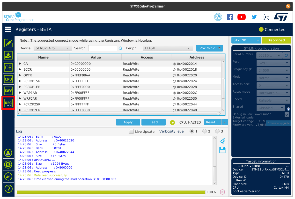
Valid FLASH Registers
| Register | Value |
|---|---|
OPTR | 0xFFEF98AA |
PCROP1SR | 0xFFFFFFFF |
PCROP1ER | 0xFFFF0000 |
WRP1AR | 0xFF00FFFF |
WRP2AR | 0xFF00FFFF |
PCROP2SR | 0xFFFFFFFF |
PCROP2ER | 0xFFFF0000 |
WRP1BR | 0xFF00FFFF |
WRP2BR | 0xFF00FFFF |
After updating the option bytes, the STM32L4R5 can now be programmed using STM32CubeProgrammer and execute firmware.
Update with STM32_Programmer_CLI
-
Apply the following commands in order:
STM32_Programmer_CLI --connect port=SWD --optionbytes RDP=0xBB STM32_Programmer_CLI --connect port=SWD --optionbytes RDP=0xAA STM32_Programmer_CLI --connect port=SWD --optionbytes nRST_STOP=1 IWDG_SW=1 IWDG_STOP=1 IWDG_STDBY=1 WWDG_SW=1 DBANK=1 nBOOT1=1 SRAM2_PE=1 SRAM2_RST=1 nSWBOOT0=01 PCROP1_STRT=0x1FFFF PCROP1_END=0x10000 WRP1A_STRT=0xFF WRP1A_END=0 WRP1B_STRT=0xFF WRP1B_END=0 STM32_Programmer_CLI --connect port=SWD --optionbytes PCROP_RDP=1 -
Verify the option byte values by displaying them to the command prompt.
STM32_Programmer_CLI --connect port=SWD --optionbytes displ -
Compare the response to the following...
UPLOADING OPTION BYTES DATA ...

  Bank          : 0x00
  Address       : 0x40022020
  Size          : 20 Bytes

██████████████████████████████████████████████████ 100%

  Bank          : 0x01
  Address       : 0x40022044
  Size          : 16 Bytes

██████████████████████████████████████████████████ 100%


OPTION BYTES BANK: 0

   Read Out Protection:

     RDP          : 0xAA (Level 0, no protection)

   BOR Level:

     BOR_LEV      : 0x0 (BOR Level 0, reset level threshold is around 1.7 V)

   User Configuration:

     nRST_STOP    : 0x1 (No reset generated when entering Stop mode)
     nRST_STDBY   : 0x0 (Reset generated when entering Standby mode)
     nRST_SHDW    : 0x0 (Reset generated when entering the Shutdown mode)
     IWDG_SW      : 0x1 (Software independant watchdog)
     IWDG_STOP    : 0x1 (IWDG counter active in stop mode)
     IWDG_STDBY   : 0x1 (IWDG counter active in standby mode)
     WWDG_SW      : 0x1 (Software window watchdog)
     BFB2         : 0x0 (Dual-bank boot disable)
     DBANK        : 0x1 (Dual bank mode with 64 bits data)
     nBOOT1       : 0x1 (Boot from system memory when BOOT0=1)
     SRAM2_PE     : 0x1 (SRAM2 parity check disable)
     SRAM2_RST    : 0x1 (SRAM2 is not erased when a system reset occurs)
     nSWBOOT0     : 0x1 (BOOT0 taken from PH3/BOOT0 pin)
     nBOOT0       : 0x1 (BOOT0 = 0, boot from system memory when nSWBOOT0=1 and main flash is empty,otherwise, boot from main flash memory)

   PCROP Protection (Bank 1):

     PCROP1_STRT  : 0x1FFFF  (0x80FFFF8)
     PCROP1_END   : 0x10000  (0x8080000)
     PCROP_RDP    : 0x1 (PCROP zone is erased when RDP is decreased)

   Write Protection (Bank 1):

     WRP1A_STRT   : 0xFF  (0x80FF000)
     WRP1A_END    : 0x0  (0x8000000)
     WRP1B_STRT   : 0xFF  (0x80FF000)
     WRP1B_END    : 0x0  (0x8000000)

OPTION BYTES BANK: 1

   PCROP Protection  (Bank 2):

     PCROP2_STRT  : 0x1FFFF  (0x81FFFF8)
     PCROP2_END   : 0x10000  (0x8180000)

   Write Protection (Bank 2):

     WRP2A_STRT   : 0xFF  (0x81FF000)
     WRP2A_END    : 0x0  (0x8100000)
     WRP2B_STRT   : 0xFF  (0x81FF000)
     WRP2B_END    : 0x0  (0x8100000)
Whichever method you used, update the STM32 MCU based boards package in Arduino IDE to the version listed in the Swan Quickstart before you program the Swan from Arduino IDE again, so the corruption doesn't recur.
Recovery documentation created based on original Blues forum post.
If you are still experiencing difficulties, please contact support@blues.com.